

The wonder material
What is graphene?
Graphene is a material made of a single layer of carbon atoms.
It has been one of the most exciting materials in recent years for a wide variety of industries ranging from electronics, energy, medicine, sensors and many more. It has been referred to as a wonder material due to its incredible mechanical strength, lightness, flexiblity, optical transparency and impressive semiconductor properties (of both electricity and heat).
Production methods have previously impeded the commercialisation of graphene, but Paragraf’s novel technique will be able to change this.
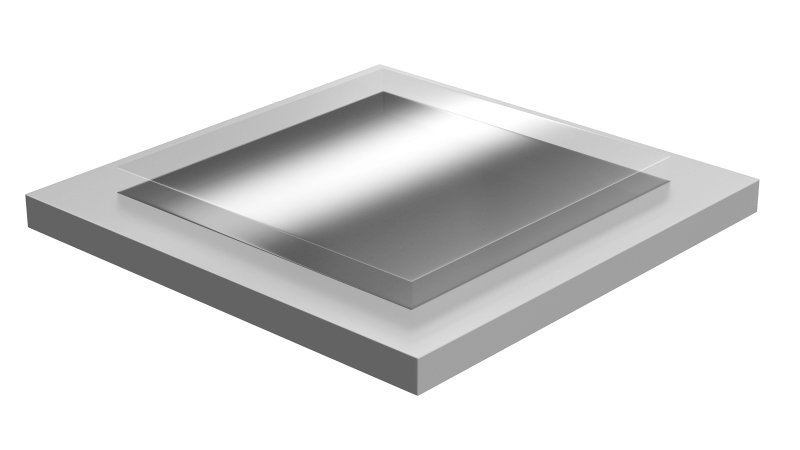
The new
beginning
with high-purity 2D graphene
at wafer scale

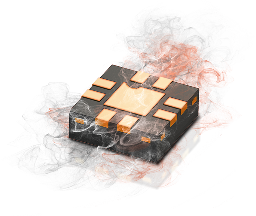
At Paragraf, we have developed a proprietary contamination free process using MOCVD (Metal organic chemical vapour deposition – a variant of CVD) to produce high-purity 2D graphene at wafer scale for the first time. This significant breakthrough delivers a high-performance graphene that is compatible with today’s production techniques and is importantly, commercially scalable. A true game changer.
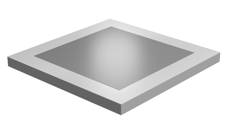
Our patented process
enables high-purity 2D graphene to be produced in a uniform layer directly onto the semiconductor-compatible substrate, eliminating the issues seen with previous techniques.
This means our high-purity 2D graphene is
- Free of residual metal atom contaminants
- Has high material uniformity
- Produced highly reproducibly at scale
- Directly made on commercial substrates used in electronic devices
Now, graphene has real potential to enhance or even directly replace standard materials in many electronic devices, moving us to a future where graphene products are mainstream.
Graphene’s potential realised by Paragraf
Paragraf’s patented manufacturing process (using MOCVD) enables the production of high-purity 2D graphene which is/has


Why hasn’t graphene taken over the world?
Despite the impressive small scale laboratory experiments showing what graphene can do and the resulting speculations about how it can change the world as we know it, it hasn’t yet. Until Paragraf, graphene production methods were either not scalable, or they impacted the purity of the graphene.
Method One – Exfoliating Method
The first is by “exfoliating” graphite. This was pioneered in 2004 and used sticky tape to remove carbon molecules from a graphite block. This method only allowed the production of very small areas of graphene which were made up of, in most cases, multiple layers of carbon, resulting in a graphene that lacked homogeneity (also known as consistency), and could not be customised or scaled, making it commercially impractical.
Method Two – CVD Method
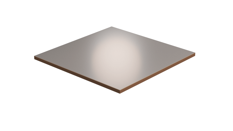
The second and larger area production method (Chemical Vapour Deposition – CVD) is the deposition of carbon molecules onto a metal substrate such as copper foil. The carbon layer is then transferred onto an electronics-compatible substrate, such as silicon, allowing it to be incorporated into electronic products. The various wet and dry processes involved in CVD result in copper atoms being left behind on the graphene during the transfer process and the graphene fracturing, affecting its purity, performance and again its commercial scalability.
CVD Method – Step 1
Graphene grown on copper using CVD
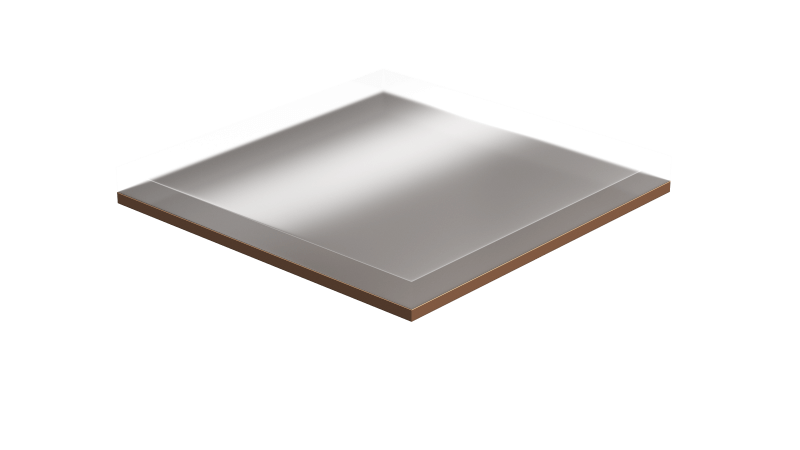
CVD Method – Step 2
Graphene coated with PMMA
CVD Method – Step 3
Copper etched away, leaving
graphene attached to PMMA

CVD Method – Step 4
Graphene and PMMA ‘transferred’
to working substrate
CVD Method – Step 5
Final Product – PMMA removed to
leave graphene attached to working
substrate
Given these shortcomings, graphene has been unavailable in a pure form and in a way that is scalable with commercial viability, hence why graphene hasn’t taken over the world yet.
Let’s work together
At Paragraf we believe in collaborating with our customers to achieve the best outcomes with our graphene-based technologies and devices.
Please get in contact…