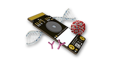
The integration of graphene into the semiconductor industry requires a deep understanding of how this material behaves, how to manipulate it in a fabrication environment and how to employ existing processes to maximise the unique properties of graphene. The commercial nature of the semiconductor industry dictates that these technical challenges need be met and overcome in a viable way that offer a significant performance advantage. Paragraf is at the forefront of making this a reality.
John Tingay, CTO, Paragraf
The properties of graphene and its potential use has occupied engineering minds for a decade and a half. Apart from its tensile strength, its conductivity is an order of magnitude higher than copper and its thermal conductivity surpasses any other material currently used in engineering. These attributes from an allotrope of carbon at just one atom thick. Manipulating graphene in a way that is compatible with standard fabrication processes could be the first significant waypoint in fully exploiting these properties in the semiconductor industry. Paragraf has successfully developed a deposition process that enables just that. We have proven the technology through the development and volume production of the world’s highest performance Hall Effect sensor.
Attention is inevitably turning to how graphene can be further integrated into the semiconductor ecosystem. The goal here is to use graphene in ways that complement existing materials, processes, and equipment. It needs to be disruptive to the target markets, rather than attempt to disrupt the entire manufacturing supply chain. It is the economies of scale that make semiconductor devices commercially viable, and graphene needs to fit into that model to effect transformation; not change the model to suit its own methods.
This is perhaps an even greater challenge than developing a way to produce graphene as a two-dimensional material. Paragraf has successfully achieved the fabrication of graphene and is now working on ways to bring its technology to the wider semiconductor industry.
The solid-state device
Perhaps the end goal here is to create large scale integrated logic devices based on a graphene transistor. That would move the needle on processor design so far that we could achieve higher clockspeeds with considerably lower heat loads. There are many researchers working on this, Paragraf included, but realistically the many and wide-ranging technology blocks needed to realise this vision is still a significant way off.
However, the wider use of graphene in solid-state devices is very much happening now. The Hall effect current sensor proves that. Making graphene another stage in standard silicon fabrication processes is where the immediate opportunities exist. These solid-state devices will exploit graphene’s known properties, using it in place of other materials, or in conjunction with device structures shown in basic research to open new product areas for the integrated device manufacturers.
Some of the most speculated topics for early areas of graphene adoption in electronics have been to overcome challenges in thermal management by increasing conductivity and providing high thermal conductivity. It is important to also point out that graphene has other useful properties: it does not cause contamination in silicon processes; it is virtually impervious to electro-static discharge (ESD), and it is inherently radiation-hard. This makes it ideal for use in integrated devices that are exposed to harsh environments and ionising radiation, not least those being used in the space industry.
The possibilities with graphene
Two trends underpin the semiconductor industry’s long history in logic until the early 2000s; higher frequency of operation more functionality on chip or in package. The integration trend is relatively simple; it delivers more functionality at a lower package cost. The package complexity is slightly more nuanced and has implications to other parts of the architecture. Higher clock frequencies mean logic circuits operate faster but combined with more integration puts increased demand on data transfer. Graphene can facilitate improvements here too.
The modulation of RF energy is key to modern communications. The roll-out of 5G cellular networks, and ultimately 6G will see these systems operating further up the frequency spectrum. This is a major step forward, because it enables the higher data rates supported by the hardware at either end. It is this move to higher frequencies that will support very high download, and potentially upload, speeds with mobile broadband and Wi-Fi. However, even this will not satisfy tomorrow’s appetite for speed. Other trends, including autonomous vehicles, will demand huge, possibly dedicated bandwidth allocations, which will continue to put service providers under pressure to strive for higher network speed, bandwidth and capacity.
This will see a move into the THz part of the spectrum. Today, the devices used to modulate and receive signals in the THz frequencies are large, expensive, complex and altogether unsuitable for mass deployment. Graphene can enable these issues to be addressed.
There have been numerous examples in the literature of THz receivers made from mechanically placed flakes of exfoliated graphene or of advanced modelling that show high performance as a THz device. The manufacture of these devices would require the integration of graphene deposition, lithography, and etch with other semiconductor processes, but would result in capabilities to enable communication into the THz band and beyond.
Graphene is well suited to optical devices. Its optical absorption can be controlled across wavelengths from visible to IR, making it applicable to receivers. With the high electron mobility of graphene means it can be used to make structures for modulators, particularly suitable for silicon photonics. The ability to control the optical properties of graphene mean a single IC could integrate both light modulation and detection, which could lead to the development of new types of silicon-based optical ICs for high bandwidth communications.
The opportunities today
Modelling and laboratory experimentation has shown the potential of graphene to surpass existing device performance. Academic teams are actively exploring the way graphene can be used in solid-state devices, often using graphene flakes to develop an example with poor reproducibility. The challenge is to take these proofs of concept devices and scale them up to wafer level. This transition can only occur with a well understood toolbox, not just the production of graphene but understanding how its properties can be controlled and modified through subsequent processing steps.
The way graphene can be incorporated, based on using existing fabrication processes, is key here. Paragraf is researching ways to extend or modify these processes in ways that allow graphene to enhance and improve integrated devices.
Conclusion
It is tempting to suggest that graphene can improve every part of the semiconductor industry. It is without doubt disruptive and may well eventually be a standard part of the logic IC design and manufacturing process. However, in the nearer term it will be applications such as THz devices, modulators and field emitters where graphene will likely be most influential and first released as a commercial product. Paragraf expects to be testing devices like these with partners within the next two years.
In that same timescale, it is predictable that some niche graphene transistor-based applications will also emerge, focussed on high frequency operation but also taking advantage of other properties of graphene, for example its high temperature stability, radiation hardness and mechanical strength. Of course, any development needs to be commercially viable, it is here that Paragraf is playing the major enabling role.


